
Aktuelles
-
 Neues Paper in Advanced Energy Materials veröffentlicht
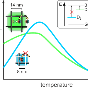
Das ist das Ergebnis einer Kollaboration mit der Gruppe um Maksym Kovalenko (ETH Zürich) zu dem Thema Exzitonendiffusion in Nanokristallanordnungen.
-
 Neues Gruppenmitglied
Bastian Schubert startet ein Praktikum in unserer Gruppe.
-
 Neuster Doktor der Arbeitsgruppe
Michael Lichtenegger verteidigte erfolgreich seine Dissertation "Exciton Diffusion in Perovskite Nanocrystal Assemblies"


Die Forschungsgruppe Nanospektroskopie


